Exhibition introduction
Creating New Possibilities in the Face of Ongoing Challenges!
Until the late 1940s the word “semiconductor” was a specialized term for a material that could not be used to precisely control circuit switches. Nowadays, almost all electronic products in daily life contain semiconductors. The computational power yielded by semiconductors marks an incredible advancement in human history, and interdisciplinary collaboration is a wonderful and fascinating aspect of semiconductor development. Scientists, engineers, manufacturing experts, supply chain specialists, marketing managers, and others in the field have contributed their expertise, manufacturing technology, and business thinking, working together and dividing up the labor to accelerate the innovations of the future.
Produced in 1961, the first silicon chip contained only four transistors. Now in 2023, a high-end smartphone processing chip contains over ten billion. The circuit patterns are smaller than the radius of the SARS-CoV-2 virus (about 50 nanometers). The numerous tiny cells function in a complex network, executing intricate computational tasks. Looking back over the history of semiconductor development, it can be seen that as innovative technologies rapidly evolved according to Moore’s Law, remarkable achievements in technology and manufacture took place in a closely intertwined global “coopetitive” relationship.
For this exhibition, we have created a research and development center, and we invite you to explore four settings — the Exhibition Hall, Materials Room, Manufacturing Zone, and Future Lab. In these spaces, you can use a range of narrative axes, artistic creations, games, and workshops to learn about and reflect on how semiconductors have changed history and shaped the future using fundamental scientific principles in ongoing innovation and collaboration. Let’s get stuck in!
Area Introduction
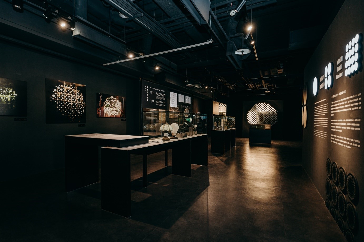
Exhibition Hall
This area is planned to be a science and technology art gallery that changes exhibits every two years. The current exhibit is from LuxuryLogico’s classic work " Solar " and a review of each production stages of the work; the same area also displays the actual integrated circuit and a series of electron micrographs which arouse the audience's curiosity about the unknown appearance.
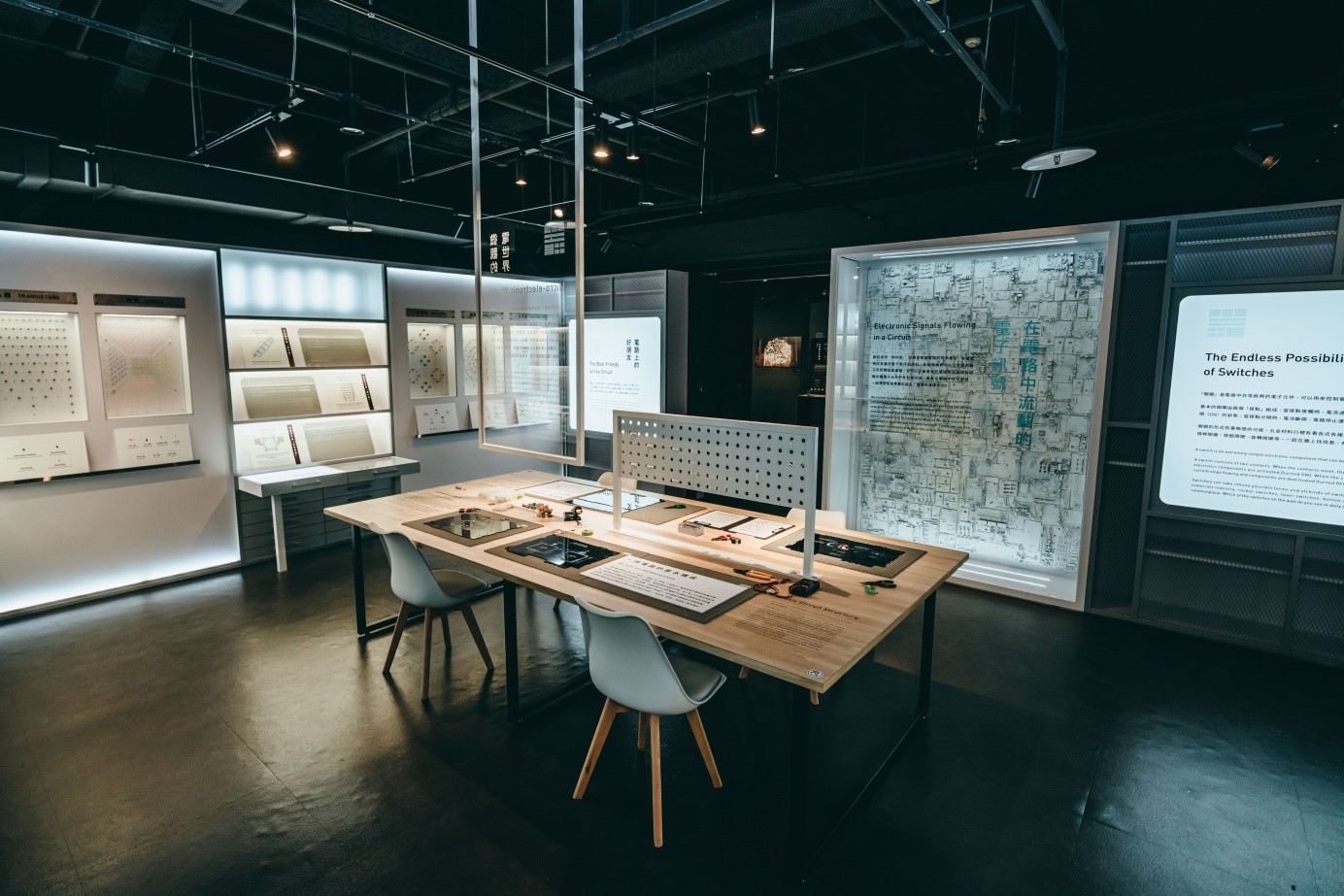
Material Room
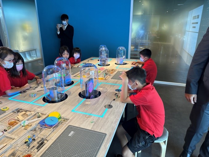
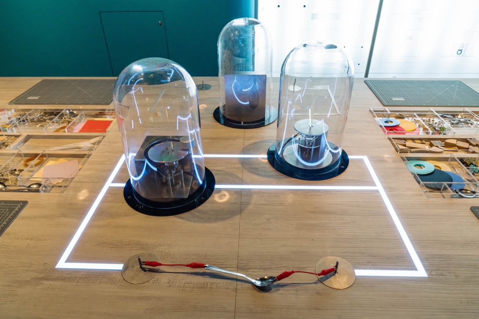
This area is set up as the material preparation room of the R&D center. The content starts with the electromagnetic knowledge of atoms and electrons, uses the analogy of a water flow system to introduce the basic structure of circuits and various discrete electronic components, and finally focuses on switches and binary bits, and how logic gates became the basis of integrated circuits.
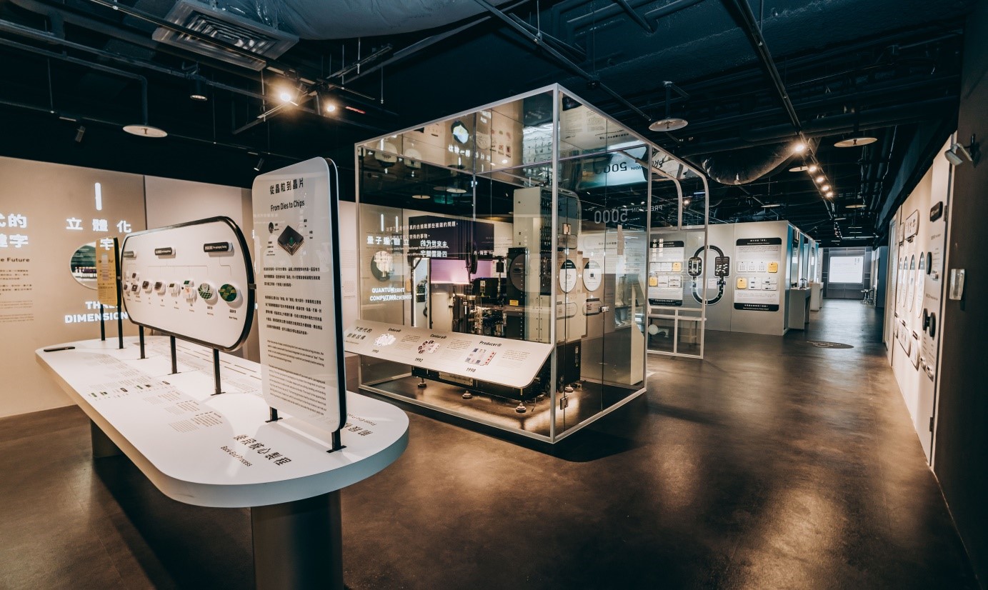
Manufacturing Zone
This area is set as the production and manufacturing base of integrated circuits. The content starts from the characteristics of semiconductors and directly cuts into the current state of the industry at the forefront. It introduces the structure of the industrial chain, the manufacturing principles of front-end and back-end processes, and various classic key process nodes. Four major future research and development directions of the semiconductors are also shared, including qubits and integrated storage and computing. In this area, Precision 5000, a classic semiconductor equipment donated by Applied Materials, is exhibited simultaneously. Together with a light show and a multimedia game that allow the audience to understand how the epoch-making single-wafer multi-chamber equipment was invented.
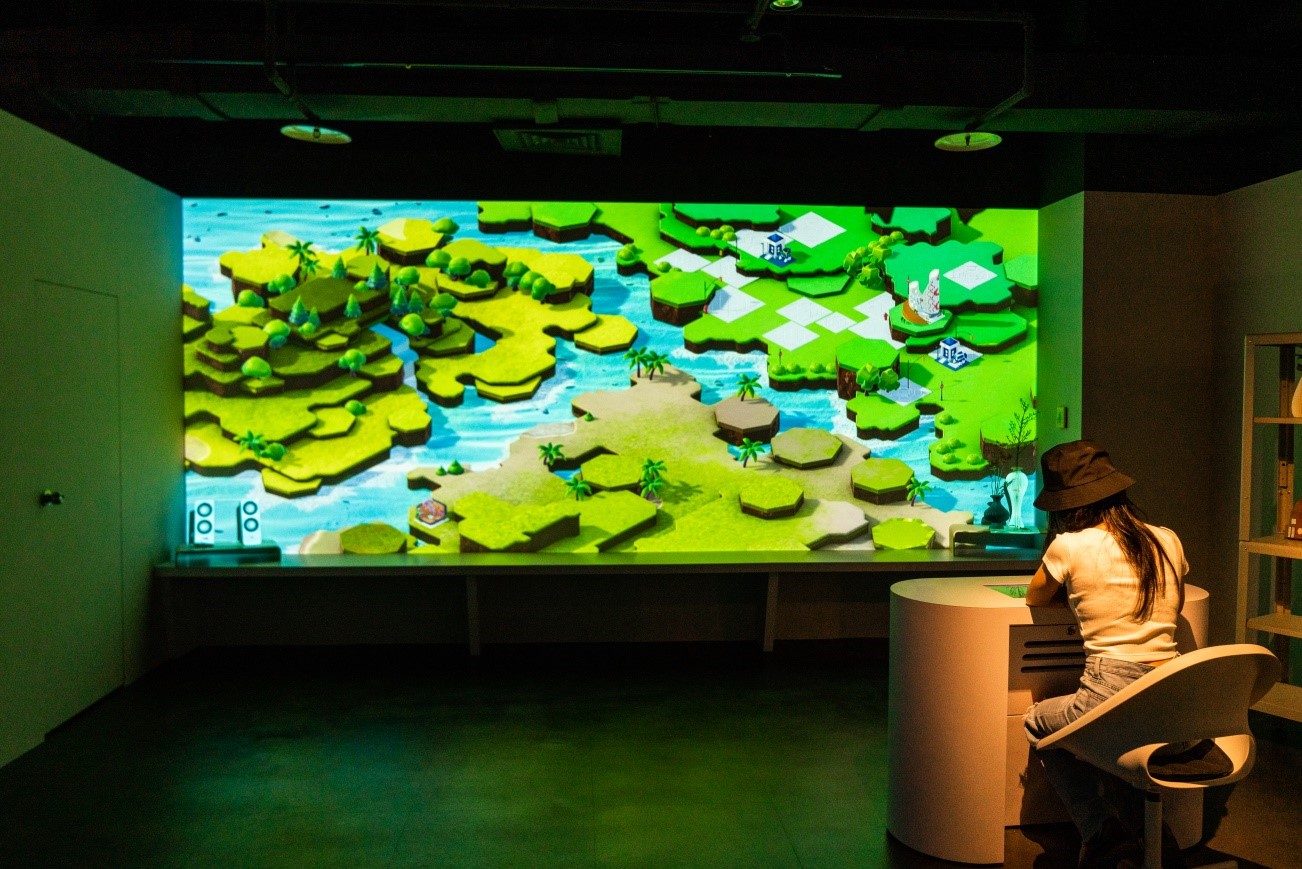
Future Lab
This area sets the situation as a remote home office in the future. Through the process of psychological tests and creative drawing, audience can complete the design challenge for the three islands with different values, and jointly create the collective future that technological development brings to us.
Exhibition Workshops
3D Circuit Workshop
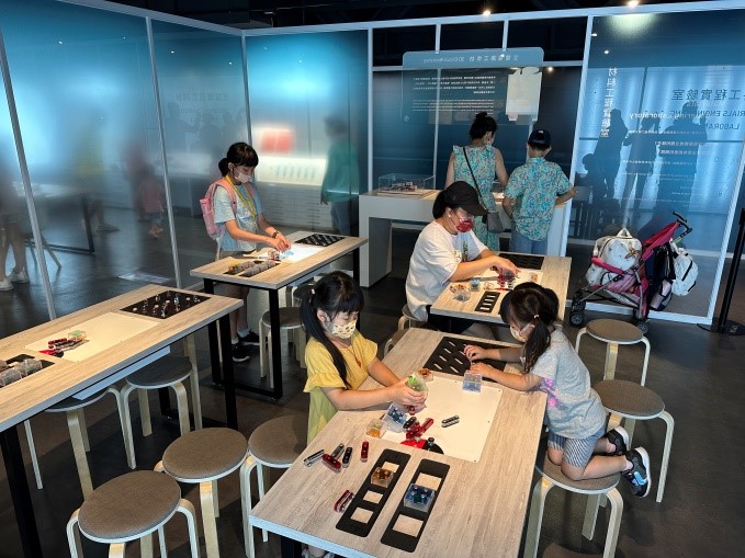
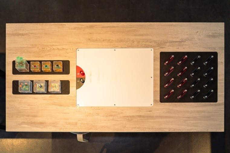
Through the newly developed component set, the audience can try to build a three-dimensional circuit system on a circuit board and understand the possibilities of 3D circuit design.
Creative Switch Workshop
In response to the popular “Tinkering” spirit, visitors can use common stationery objects as materials and try to design a creative switch that can drive the operation of the model.
Technological development is driven by human needs. In the early twentieth century, the invention of vacuum tubes propelled the development of radio, long-distance call, radiotelegraphy, radar and computer; however, as vacuum tubes are large and energy-consuming, Bell Laboratories created the ever-smaller transistor during World War II as a replacement. Later, due to the increasing necessity for smaller, thinner and lighter electrical devices, the integrated circuit was born. Over the last fifty years, electronic components have evolved from minimeter- to micrometer- and nanometer-sized scales; space needed nonetheless, their performances have increased significantly despite the size reduction. The information industry has also transformed from PC and Internet era into the new era of intelligent mobile devices, foreseeing an explosive evolution.
Einstein once said, “Imagination is more important than knowledge.” Going through the three phases of vacuum tubes, transistors and integrated circuits, the evolution of the semiconductor can be best described as boundless imagination and infinite dreams of technology. Corresponding to the characteristics, applications and evolution of semiconductors, the exhibition consists of five themes: Atom Playroom, Discovering Bell Labs, Micro-world Exploration, Photoelectric Dream Factory and Infinite Future and Beyond. With the help of multi-media and mechanical devices, visitors can explore the fascinating world of semiconductors through interactive gaming.